
How it is made : Nintendo Switch game cartridge

Before talking about the resilience of the games against any form of piracy, let’s discover what stands inside the game package.
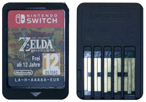
The cartridge itself is small and exhibits 16 connections to the console on what appears to be a PCB. The first step of this teardown is to open the cartridge to further assess its construction.

Opening the cartridge is fairly easy and can be done with a scalpel for example. Once opened, a single chip is visible with the PCB visible from the outside being part of the chip.
The chip is labelled with the manufacturer name being MXIC and have a number of reference.


Few drops of hot fuming nitric acid can be used to create a partial opening on top of the chip.
From that point, a cross section of the entire package can be done on the same sample or on a new one to keep the result clean.

This package cross section shows that the package internal PCB is made of two layers that can be made visible by using a fine abrasive and « polishing » its bottom layer to make the second one visible. In that process, the intermediate layer with via connecting both PCB layers can also be made visible.

Using Nitric acid to create a partial opening is etching copper away. In that particular setup, the bonding wires that connects the two chips together and to the PCB would also be etched away if Copper made. This is obviously not the case which indicates gold bonding wires.

As a funny fact, the bonding wires do not connect the two chips directly. The « security » module as well as the main memory has their bounding pads on one side but those two sides are not facing each other which result in the bonding wires being connected to the PCB that routes the signals underneath the main memory.

Using more nitric acid can be used to dissolve the remain of the package and get the naked dies.
From this point, the two chips can be studied through Reverse-Engineering to give their secrets away.
It is pretty easy to guess the strategy pirates would use to create counterfeited games. Some assumptions can be made at this early phase of the study. The memory can be either ROM or Flash based. This can be easily verified by etching the chip interconnections and looking at the patterned silicon.
The memory can use a proprietary protocol which would require a custom chip design which would not be necessary and would add an extra cost for the design and manufacturing.
It is also likely that the chip is a standard flash storing encrypted data. In this condition, the second chip would be used to decrypt data on the fly when needed.
To further protect their IP, the « security » module can also be used to authenticate the game when plugged to the console. Therefore, it would serve a dual purpose : authentication and decrypting.

From this point, this « security » module would become the main target for a counterfeiter. Reverse-Engineering can then be used to extract its firmware and potential cryptographic keys. With that knowledge and assuming the attacker can emulate the authentication protocol and the decryption algorithm on a publicly available micro-controller, a counterfeit product could be design.
Of course, at this stage of the study, it is impossible to conclude on the different aspects discussed here.
If you want to know more, discover the corresponding Chip ID that goes into more details with cross sections of the package and chips, pictures of the PCB layers, top optical scans of the chips, visible die marks, substrate optical scans and SEM close up showing the system in greater details.